


Building the Bridge: India-Japan Semiconductor Cooperation at Semicon Setu 2026
On 19 September 2026, "The Semicon Setu 2026": a closed-door business seminar at Yashobhoomi, New Delhi, held as part of Semicon India 2026, convened by Japan India Business Bureau (JIBB) . Delegates from Japan and India spoke across the session on semiconductor investment, collaboration, and the shape of an emerging bilateral ecosystem. What stood out was how little the conversation resembled the diplomatic set-pieces typically associated with India-Japan relations. Instead of strategic autonomy or balancing behaviour, the room discussed capex subsidies, polymer removal chemicals, and land parcels in Yamuna Authority. This is, in some sense, the texture of contemporary India-Japan relations - high politics translated into procurement decisions.
The National Architecture Behind the Pitches
The state and company presentations at Semicon Setu sit inside a larger policy structure that had just been reinforced weeks earlier. Union Budget 2026-27 introduced the India Semiconductor Mission (ISM) 2.0, with a provision of ₹1,000 crore for the year and an emphasis on domestic production of semiconductor equipment and materials, full-stack Indian chip design and stronger supply chains. This builds on the Cabinet's approval of the broader Semicon India Programme 2.0, carrying a fiscal outlay of ₹1,27,500 crore across six pillars: design of chips, machines and materials, setting up more fabs, strengthening the ATMP/OSAT industry, research and development, and talent development.

Total investment committed under the mission stands near 18 billion US dollars, and the domestic semiconductor market, valued at roughly 38 billion dollars in 2023, is projected to reach 100 to 110 billion dollars by 2030, with a roadmap targeting 3-nanometre and 2-nanometre nodes by 2035. Set against this backdrop, the state pitches and company presentations at Semicon Setu are the ground-level expression of a centrally coordinated push, with states and firms filling in the specific slots the national mission has opened.
Moving from Statecraft to State Incentives
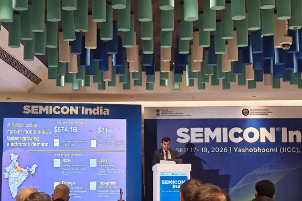
The presentations from various states such as Uttar Pradesh, Karnataka, and Odisha illustrated how India's federal structure has become an active site for semiconductor diplomacy. UP's pitch centred on proximity to the National Capital Region (NCR), the Jewar air-cargo gateway, an existing design industry base around Noida and land readiness for fabrication-grade projects. Dedicated Japanese, Korean, and Taiwanese cities (industrial townships) being carved out under the Yamuna Expressway Industrial Development Authority (YEIDA) were also mentioned. Additionally, roughly 75,000 acres are earmarked by the Noida Industrial Development Authority for allotment through the Nivesh Mitra single-window system. The intention is to build a full-stack design ecosystem anchored in Noida rather than a single fabrication plant surrounded by empty land.

Odisha's presentation offered a different register. The state's trajectory was framed as a shift "from mine economy to mind economy," pairing its established strength in minerals and metals with claims to some of the cheapest power tariffs in the country and a young talent pipeline. The state cited a ten-fold rise in gross state domestic product since 2005-06 and a spot among the top five states in investment friendliness. Whether these figures translate into fabrication investment or remain confined to assembly, testing, and packaging work is a question worth watching. The map of approved plants shown during the session listed Odisha's Bhubaneswar cluster as host to 3D Glass and SicSem, alongside Gujarat's more established Sanand and Dholera clusters and Uttar Pradesh's HCL-Foxconn facility in Noida.

The broader status slide was worth pausing on: twelve plants approved nationally, three already in production. Against the scale of India's semiconductor ambitions, that is still an early stage, though the geographic spread, from Punjab's Mohali to Assam's Jagiroad, suggests the mission is deliberately distributing capacity rather than concentrating it in one or two states.
Where Japan Fits
The Japanese side of the room spoke more about specific technical niches. A presentation on Mie Prefecture described it as home to one of Japan's established semiconductor clusters, with Yokkaichi serving as a centre of semiconductor manufacturing employment. Associated with Mie University, professor Hideto Miyaki, spoke on deep-ultraviolet LED work involving high-quality aluminium nitride and sapphire substrates, connecting this materials research to the wider Nagoya region's industrial base. This was a reminder that Japan's contribution to the relationship includes decades of accumulated expertise in materials science, equipment and process know-how.

KISCO India's presentation made this concrete at the level of the supply chain. The company positioned itself as a materials specialist offering bonding wires, mould cleaning solutions, solder balls, and surface treatment chemicals, with existing relationships to firms such as TSMC and PSMC. Its focus market map placed Delhi, Gujarat, Mumbai and Pune, Bangalore, and Chennai as priority zones, each tied to a different downstream use, from electric vehicle components to raw materials for pharmaceuticals and cosmetics.
It also positioned itself as a conduit for Chinese and Taiwanese suppliers seeking Indian customers, which is a useful corrective to any account of India-Japan semiconductor cooperation that treats it as a purely bilateral affair. In practice, this cooperation is triangulated through Taiwan's manufacturing dominance and China's supply chains as much as it runs directly between New Delhi and Tokyo. This was visible in the architecture of Semicon India 2026 itself, held under the theme "Silicon to Systems: Building the Ecosystem" and drawing over 600 companies from 52 countries.
The Japan Pavilion: Framework to Announcement

The broader Semicon India 2026 floor offered a concrete sense of what Japan's role as an industrial pillar looks like in practice. Fujifilm announced an ₹800 crore investment in a greenfield semiconductor materials facility in India, to be built in two phases, with commercial production targeted for fiscal year 2028. Hirata Corporation entered the Indian semiconductor equipment market through an exclusive distribution partnership with Hyderabad-based ATS India, extending a decade-old relationship in the automotive sector into wafer-handling robots and equipment for backend and OSAT operations. Tata Electronics and Sumitomo Chemical signed a memorandum of understanding to supply photoresists and high-purity chemicals, such as hydrogen peroxide and sulfuric acid, to Tata's upcoming fab in Dholera, Gujarat, with a further agreement to explore manufacturing these materials in India rather than only importing them, a fab that already draws on Taiwan's PSMC for its process technology portfolio.
These announcements were made across the wider Semicon India floor rather than inside the Setu session itself, part of the same broader push toward deeper collaboration

This is not a new dependency. Japan has long held a quiet dominance over the upstream layer of the global semiconductor supply chain that rarely makes headlines the way fabs do. According to a 2024 Brookings Institution analysis, Japanese firms hold an 88 percent global market share in semiconductor coater and developer equipment, over 50 percent in silicon wafers, and roughly half of photoresists, segments led by firms such as Tokyo Electron, Shin-Etsu Chemical, and JSR. What KISCO and Hirata are each doing in India, in their own smaller ways, is extending this pre-existing Japanese dominance in materials and equipment into a new geography, one node in a global structure rather than a bilateral arrangement built from scratch.
Alongside Japan, the event hosted dedicated Country Pavilions for South Korea, Malaysia, the Netherlands, Singapore, and Sweden, each representing a different layer of the value chain: South Korea's memory dominance through Samsung and SK Hynix, Malaysia's roughly 13 percent share of global assembly, testing, and packaging, and the Netherlands' presence through ASML, whose monopoly on extreme ultraviolet lithography machines makes it indispensable to chip manufacturing at the most advanced nodes. Japan's own pavilion, and its presence at Semicon Setu, sat inside this wider field rather than beside it. Cooperation of the kind on display at the Setu session is India's entry point into one corner of a structure assembled from several such national specialisations, not a standalone bilateral relationship.
The Framework and What It Omits
The session also included a slide titled "Japan-India Collaboration Framework," which divided the relationship cleanly: Japan supplying technology, equipment, materials, and know-how; India supplying talent, market growth, and manufacturing expansion; the two together building a globally competitive semiconductor ecosystem. The announcement that a Japan-India SETU Forum will convene in Tokyo on 10 December 2026 suggests the gaps such as financing structures, intellectual property protection and the workforce training needed to make talent claims credible at scale, are recognised, and that the relationship is meant to continue in structured, recurring form rather than as a series of one-off seminars.
What will determine whether Odisha's "Mind Economy" or Noida's design ecosystem actually take shape lies in decisions made by state investment authorities, materials suppliers and mid-sized manufacturing firms rather than in the language of summit diplomacy. What the framework slide compresses into a single exchange of technology for talent is, on the ground, something closer to resilience assembled through complementary capabilities: a Japanese materials firm supplying both Indian EV and pharmaceutical sectors from the same production line, a Taiwanese supplier reaching Indian customers through a Japanese intermediary. This type of system is precisely what is built one commercial relationship at a time, and the Semicon Setu and the broader ‘Semicon India 2026: Silicon to Systems’ was a rare chance to watch that process from inside the room.
About the Author
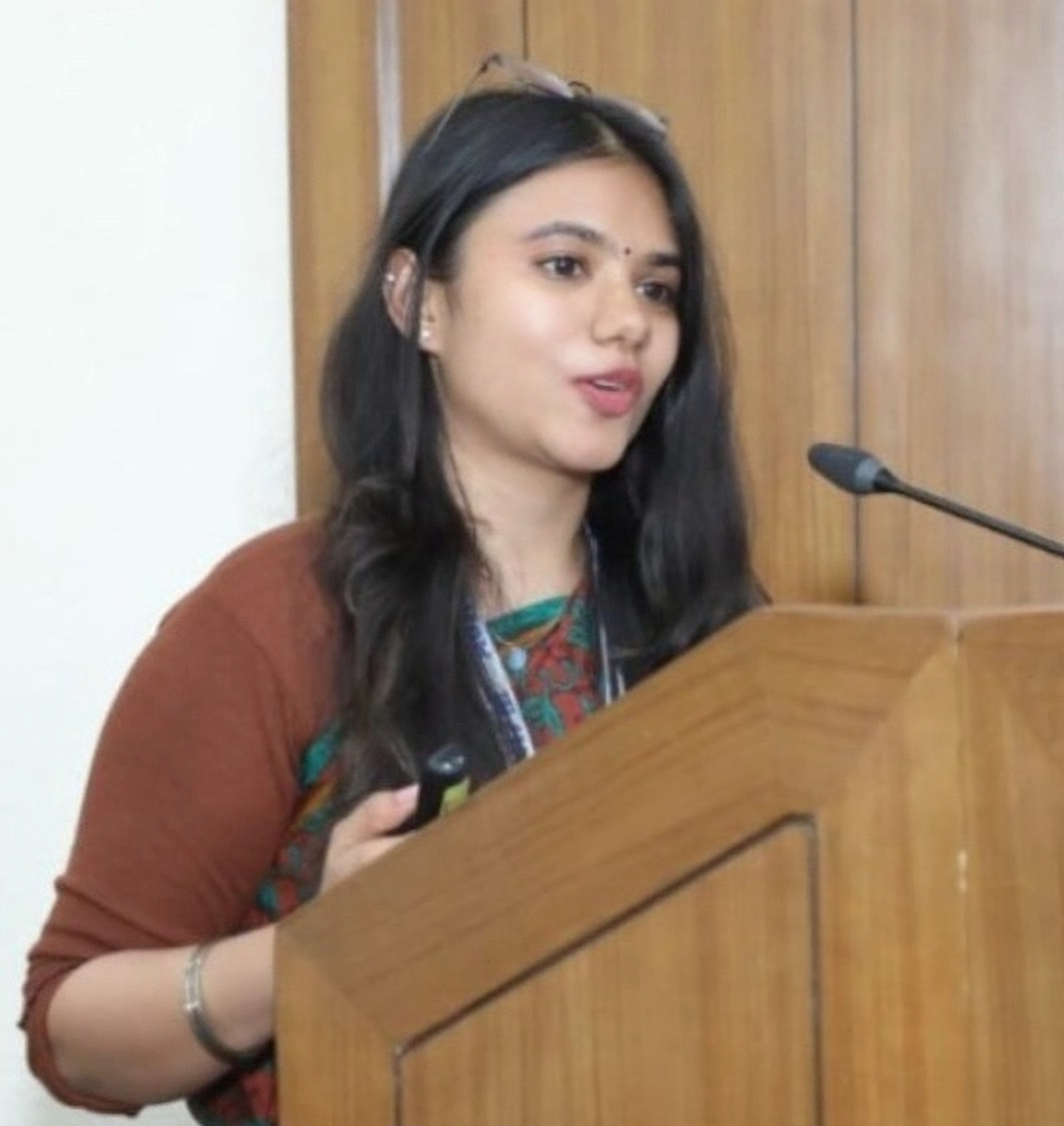
Kaveri Jain is a doctoral researcher in International Relations at the Amity Institute of International Studies, Amity University, Noida. Her work focuses on India-Japan relations during the Shinzo Abe era. She has presented at academic conferences, published in peer-reviewed platforms and written on various aspects of India-Japan ties, including foreign policy, technology cooperation, cultural exchange, diaspora diplomacy and engagement in the Indo-Pacific region.


Comments